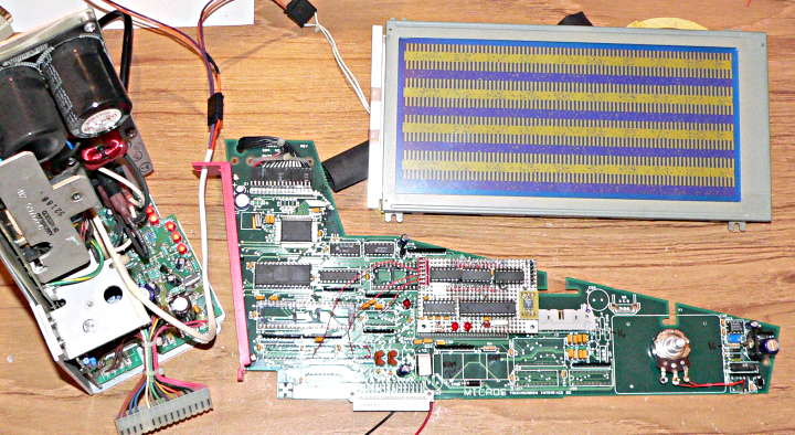
Years ago, around the time DorkbotPDX's meetup moved from Vendetta to NW Lucky Lab, Ben Bleything brought LCDs from decommissioned point-of-sale terminals to the meetup. I did some reverse engineering to get them working!

At the time, I wrote 3 blog articles aboug the reverse engineering effort. Only one of them survived from the early days of this website. Recently, I found the original text those old 3 articles, and also a small pile of the LCDs... which I'll be giving away at upcoming meetings!
Click "Read more" for those 3 original articles with the fine details of reverse engineering (and source code) for these old LCDs....
Blog #1 - Reverse Engineering the LCD
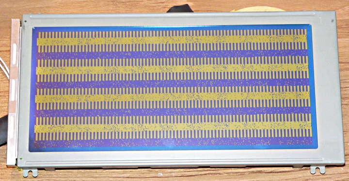
Last nice Ben brought a Micros 2700 POS terminal to the meeting. Here is one of the LCD screens:
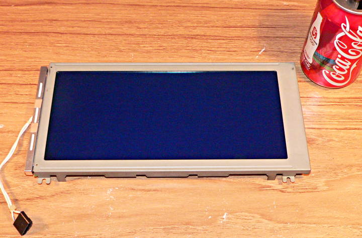
The LCD is a Emerging model EG64E00BCWU (nice of them to put a sticker on the back side with the model number). Here is a datasheet for the LCD:
http://www.pjrc.com/tech/eg64e00bcwu/eg64e00bcwu.pdf
(this PDF file is attached below, in case this link ever becomes 404...)
Yes, it's 640 by 200 pixels with a CCFL backlight!
Unfortunately, the LCD doesn't have the controller chip (with nice interface) with a frame buffer built on board. It's on this similarly large card.
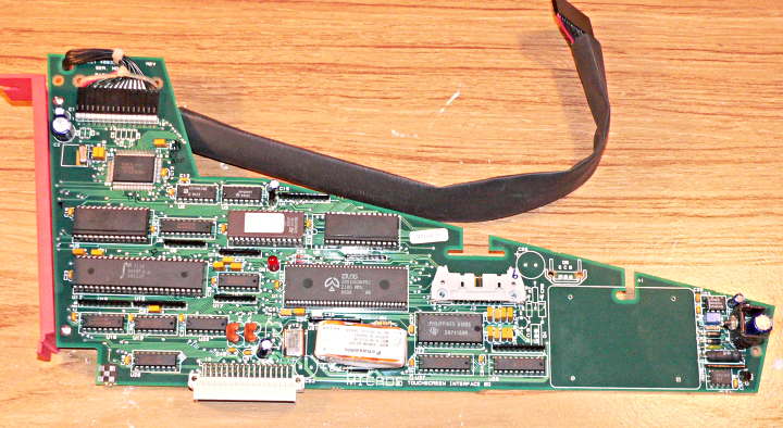
The QFP chip in the upper right (U1) is the controller chip. It's made by OKI and has "M6255" printed on it, which at first seems to turn up only datasheets for opamps. It turns out the part number is actually "MSM6255", and here is the datasheet:
http://www.pjrc.com/tech/eg64e00bcwu/msm6255.pdf
(this PDF file is attached below, in case this link ever becomes 404...)
The frame buffer memory isn't built in to the chip. That 28 pin part right below it seems to be the frame buffer memory. The MSM6255 has 2 busses (both 8 bit data, 16 bit address), one which connects to the frame buffer memory chip and the other to the CPU's memory.
That big chip in the center is a Z80 processor, and the two memory chip above it appear to be the firmware and RAM it uses. The big chip right below the frame buffer memory is a IDT7132 dual-port RAM chip, which I believe the designers used to communicate between this Z80 and the main Z80 that runs the rest of the terminal (together with several other Z80s). But really, who cares about that? I just want to figure out how to scrape all that stuff off and get access to the display....
So, with a printout of the MSM6255 pinout, I started tracing out where signals connect. The Address and Data busses are pretty straigtforward. I didn't trace the to the Z80 and dual-port RAM, though I'm pretty sure they go there. My intention is to pull all those chips off and drive the bus with my own micro.
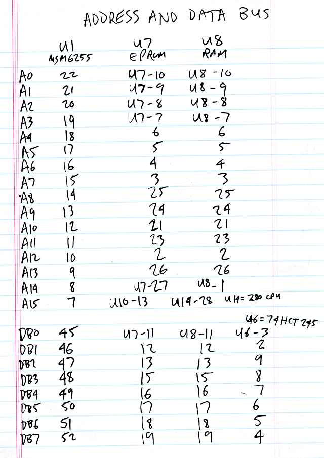
Tracing the control signals is harder. They are connected to pullup resistors, so all over the place my meter auto-ranges from megaohms down to kiloohms, which makes the process so slowly. Anyway, here's what I've learned so far.
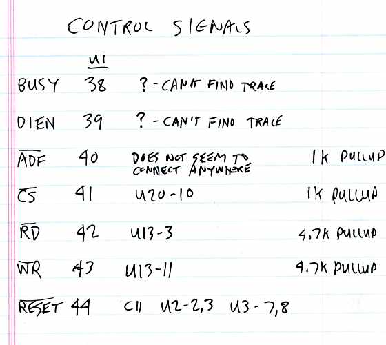
It also seems not all the power pins of all the chips are connected together. The LCD and its frame buffer, for example, do not connect to the same power as the Z80 and its memory.
More to come....
My hope is to get this thing working with a AVR, so everyone (who gets one from Ben) can play with one of these huge screens.
Blog #2 - LCD Almost Working
I'm getting close to making the LCDs work from Ben's Micro 2700 POS terminals (several of them are still up for grabs). Here's a photo.
More photos and technical details below...
First, I cut out almost all the chips. Here's a photos taken before I chopped all the chips off.
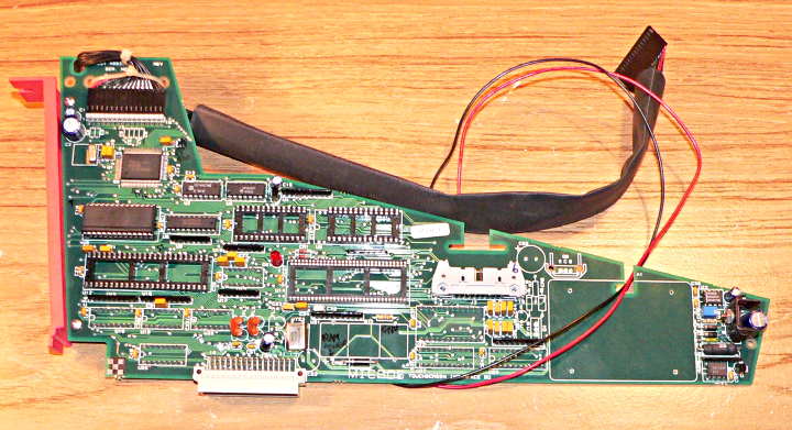
Really only 3 chips in the upper left corner are needed, the MSM6255 controller chip, the 32k RAM chip, and a 74HCT245 tri-state buffer. (those other 2 chips I left in place are buffers and transistors which seem to do startup stuff like reset pules and switching the RAM chip from battery backup to main power).
The MSM6255 has two busses, both 8 bit data, 16 bit addresses. One bus is for the Z80 microcontroller, and the other is a dedicated bus for the frame buffer RAM chip. The LCD controller only has 9 configuration registers, and a single instruction register. It only listens on 1 of the 16 address lines, which select between the instruction register or the 9 config registers. To write to the chip, you write to instruction register with A0=1, with the number of the config reigster you want. Then you write again with A0=0 to configure. Repeat this process 9 times to configure everything. However, a few of the reigsters only matter in character mode, and this board is wired only for graphical mode.
Since there are no other chips on the Z80 bus, I just wired the LCD controller chip select low (fount at U20, pin 10), and then it only takes 1 write select signal (found at U13, pin 11) to strobe the data in. Of course, A0 and the 8 data lines have to correct before pulsing the write pin low.
To access the frame buffer, the is a 74HCT245 tri-state buffer which causes the Z80 data lines to drive the frame buffer data lines. The LCD controller also has an address mux controlled by the DIEN signal. Both of these fortunately are high for the controller to access the frame buffer and low when the Z80 bus drives the RAM. So I just shorted them together (found at U19, pin 2 and 11). The RAM has its read signal low all the time. All I had to do was short the RAM CS signal low (found at U20, pin 6) to allow it to work.
The RAM write signal takes priority over read, so when you want to write new data into the frame buffer, all that's necessary is to drive DIEN and the '245 enable low to connect the Z80 bus to the frame buffer RAM (of course, set up the desired address and data first), and then pulse the RAM write signal low.
The frame buffer can be written at any time this way, but if this also happens to be at a moment when the LCD controller is reading, the screen will momentarily display whatever was on the frame buffer RAM data lines being driven by the 74HCT245 buffer. It appears this is the way the Micros 2700 worked.
The datasheet gives two suggestions for detecting times when the LCD controller isn't reading the data lines, and one of them isn't practical for large displays like this one. The other basically involves watching the CH0 signal from the controller and doing the framebuffer access right after it changes. I could not find the CH0 signal routed anywhere on the board, so I'm pretty sure Micros just didn't use it (they certainly didn't build the complex flip-flop sync circuit suggested in the MSM6255 datasheet). Maybe when I've got everything figured out I'll wire CH0 to a port pin and write a bit of code that waits for it to change right before I do the framebuffer write. It looks like CH0 is about a 560 kHz square wave, so that's plenty of time for a tight loop in the 18.432 MHz AVR to detect and complete the access. But for now, I'm not worrying about CH0.
So, here's my little circuit.
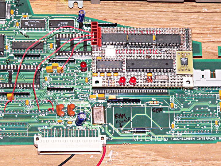
On the top are three 74HC164 shift register chips. These are connected to the MOSI and SCLK signals, so whatever the last 3 bytes were on the SPI port, they end up driving the Z80 address and data bus. The board has two headers that plug into the socket for the RAM chip that was dedicated to the Z80, so power, ground and all the address and data lines are connected there. That just leave the 2 write strobes for the LCD controller and frame buffer RAM, and the enable signal to drive the frame buffer bus. Only 3 extra signals! Well, maybe a 4th when/if I connect CH0 to avoid flicker.
The 28 pin chip is a ATMEGA88 - the same chip as the Aurdino, but only 8k of program memory. The chip on the left is a MAX232, and the white 3 pin connector is for a serial port that is intended to (someday) allow images to be downloaded easily. The little 8 pin chip on the right right is a 128K flash rom with SPI interface (Atmel AT45D011), which can hold 8 full-screem images, when I get all the pixels under control!
But not everything is working perfectly... yet. Here's what I get so far, trying to fill the entire frame buffer with 0x0F.
Those vertical bars are the desired pixels. They do change to other patters if I fill the frame buffer with other bytes. So at least I'm controlling some pixels.
Clearly, I haven't got the correct configuration for the LCD controller yet. The controller is designed to drive 2 sets of shift registers on the LCD, with 1, 2 or 4 bits per. This LCD seems to have only 1 shifter register with 4 bits, so I'm not entirely sure if I should use 2 or 4 bit mode, and exactly what the duty cycle setting should be isn't clear either. I've tried many different settings (mostly randomly), and so far none have been perfect.
I'll probably do one more session with the ohm meter to figure out more about how the LCD interfaces to the controller, and details about the frame buffer bus (which so far I've assumed is wired like the datasheet describes, but really all my probing has been on the Z80 bus and the many control signals).
Here are my latest notes/scribbles about how to connect the various signals.

I should also mention the stuff I learned about the power supply.
First, the simple part, the backlight. It's a cold cathode flourscent lamp, and there is a module inside the main power supply. It's attached to the high voltage board deep inside, and so far I've just left it alone. I did stick my meter probe in there (past all the live 120 volt stuff in the way), and it looks like that module takes 24 volts DC input. Not at nice as 5 volts, but still not too bad. It looks like it can be easily separated and liberated from the big hulking power supply. The one sad bit is there is only 1 in there, with a Y cable to drive both LCDs.... so if everyone wants one of these LCDs for a project, half of them will need to acquire or build a CCFL driver.
The not-as-simple part (but still a lot simpler than the LCD config and frame buffer bus) is the LCD drive voltage. The LCD runs on 5 volts for its logic, and a negative voltage, up to -19 volts. The parts on the far right side of the board are a little switching power supply that converts +5 into a variable negative voltage.
At first I thought the littl blue trim pot was the answer, but I kept getting very random results, especially if I touched the board. It turns out the chip in the lower right corner is a X9C103 digitally controlled pot, which adjusts the LCD drive voltage (which is what controls the contrast). I thought about hooking it up to the microcontroller, but in the interest of getting this thing to work, I simply clipped it off the board and wiring in a concention 10K pot, which you can see in the photo. However, the digital control pot is there on the board, so when/if anyone else uses all this, it's possible to control it from software. The X9C103 contains EEPROM memory to store the pot setting. I must have changed mine hundreds of times while touching the floating inputs with my fingers and wondering what I was doing that changed the LCD so much!
I had hoped to get this thing working before the next Dorkbot meeting, but it looks like I might have to put this whole thing on the shelf for a couple weeks (to make room for a paying project - which funds all this fun stuff....) I'm pretty sure I'll get the LCD config and frame buffer issues worked out, and when I do it's my hope everone in Portland Dorkbot who wants one of these displays can have one!
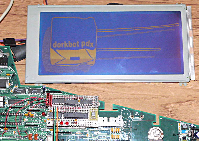
Blog #3 - LCD Working
The LCD is working! Here's a photo:
I wrote a little GUI program to load images onto the board. Here's a screenshot:

You can download everything with these links:
Gui App, Windows (flakey) - requires mingwm10.dll
AVR Firmware Source Code and mega88.asm
Small Collection of Test Images
(these files are attached below, in case these links ever become 404 Not Found...)
I picked up a few more of the Micro 2700 terminals from Ben, and they're avaialble for free to anyone in Dorkbot who wants one (and is willing to carry it home from the meeting).
The wiring is pretty much like I described in the last entry... you need 3 control signals and the bus, which has 8 data lines and 16 address lines. I used SCK and MOSI to drive 3 shift register chips, so really this entire display interfaces with only 5 pins.
Extra Unpublished Info (from email) - Detailed Wiring Description
From the mail list..
I'd love to take one of the LCDs home at the next meeting. Would I need "the big card" as well to get them running via your instructions? I'm hoping to just follow what you wrote exactly and see if I can get one displaying something for myself.
Yes, the display needs to be driven by the MSM6255 chip and its related circuitry, which is on the big card. The other stuff is a RAM chip, which holds the currently displayed image (the "frame buffer"), which is continuously read by the MSM6255. There's also a '245 buffer chip, with lets you override the MSM6255's control of the RAM, so you can write new image data into it. The display runs on +5 volts, as does the card. The display also needs a negative supply, which is produced from the +5 by the circuitry on the far edge of the card.
The motherboard has what looks like the same circuits on it, used to drive the other display. I haven't traced out of the signals on the motherboard like I did on the card, but if people use up the cards and can't figure out where to tap the signals on the motherboard, I could do it.
To use the display, you need to connect 8 data lines, 15 address lines, and 3 control signals (and short a couple signals to ground - and of course remove all unnecessary chips). Because the MEGA88 has so few I/O pins, I used three 74HC164 shift register chips connected to MOSI and SCLK to get all the address and data lines. If you used a chip like the MEGA644P with lots of I/O pins, you could probably just use I/O pins and not worry about the shift registers. Then again, there are never enough I/O pins so using only MOSI and SCLK is nice, even if it takes a little time to wait for the 3 bytes to shift out.
The 15 address and 8 data lines are all available at the socket for the EPROM or the right-most RAM chip (the one not used by the MSM6255). I built my board to just plug into the RAM chip socket to connect those 23 lines and also get power. That left only 3 wires to run to the rest of the board.
To write into the frame buffer is really very simple. You just output the 8 bit data you want, and the 15 bit address where you want it written. Then you drive the '245 enable line low to take control of the RAM chip, and then drive the write strobe low to write the data. Then rise the write line back high to complete the write, and the enable signal back high again to allow the MSM6255 to keep using the RAM normally. The buffer enable signal also connects to the DIEN pin on the MSM6255, so your 15 address lines get fed though the MSM6255 to the RAM while the buffer feeds your data to it. It's nice that they made both of them high for normal display operation and low for access to the RAM. There's also one other write strobe, which you use (without the buffer enable) to write configuration into the MSM6255 (see the MSM6255 datasheet for details, and my code for the config guesswork I did that seems to work pretty well - though other configs might be possible).
The one other thing you need to do is control the LCD negative voltage. There is a digitally controlled pot on the board. I just cut if off and wired in a normal pot, which was a lot easier for reverse engineering the display (while trying to guess the MSM6255 config settings, turning the pot back and forth and viewing from different angles could let me guess if parts of the LCD were being double-scanned from incorrect config - and believe me, I tried many incorrect settings!) If you want software control of the contrast, you might try configuring the pot? That should be pretty easy to troubleshoot since you can just measure the voltage as you try it. If you're going to replace with a normal pot, you'll need a 10K linear taper (maybe on the group order?)
I didn't draw a nice schematic (and don't plan to - but all the source code is online).... but maybe someone will draw something up to help others?