On my post about the regression test set, jeppius asked if I had sample Arduino code for these AD75019 chips.
Click "Read more" for the Arduino code and details....
First, a bit of background. The AD75019 has 256 bidirectional analog switches in a 16x16 grid. The 256 switches can connect between any X and Y pin. Here's the main diagram. The full datasheet is attached below.
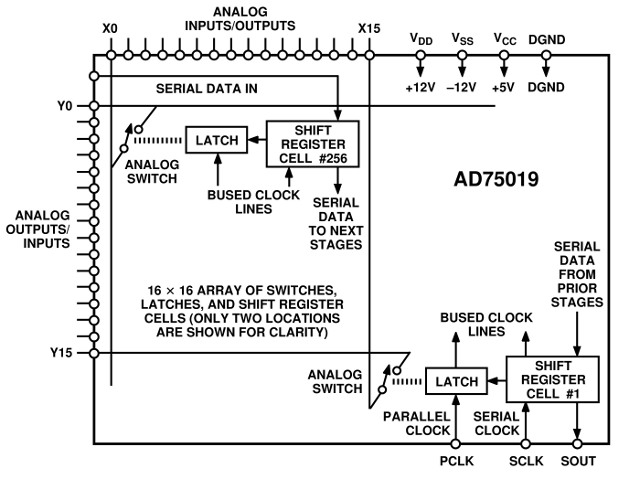
The chip is controlled by a big 256 bit shift register. I just chained the 3 chips in tandem, so the shift register is 768 bits.
In the regression tester, I used 3 of these chips to allow any combination of the 48 signals (on the X pins) to connect to any of 16 signals (on the Y pins). The 16 Y pins are connected as a 16 bit bus between these 3 chips, and the sets of 3 chips on the other boards in the tester. This "anything to the 16 signal bus" approach is important for understanging the code.
Here is the Arduino code:
// pinout
#define SCLK_PIN	13
#define SIN_PIN		14
#define PCLK_PIN	15 // only to selected board, others are high

uint8_t update_required=0;
uint16_t switches[48];

void setup()
{
	pinMode(SCLK_PIN, OUTPUT);
	pinMode(SIN_PIN, OUTPUT);
	digitalWrite(PCLK_PIN, HIGH);
	pinMode(PCLK_PIN, OUTPUT);
}

void loop()
{
}

///////////////////////////////////////////////////////////////////////
//
//   AD75019 Switch Matrix Control
//
///////////////////////////////////////////////////////////////////////

// connect a Teensy pin (0 to 48) to a bus signal (0 to 15)
void connect(uint8_t pin, uint8_t signal)
{
	uint8_t chip;
	if (pin < 16) chip = 32;
	else if (pin < 32) chip = 16;
	else if (pin < 48) chip = 0;
	else return;
	if (signal >= 16) return;
	switches[chip + (15 - signal)] |= (1 << (pin & 15));
	update_required = 1;
}

void disconnectAll(void)
{
	memset(switches, 0, sizeof(switches));
	update_required = 1;
}

void update(void)
{
	uint8_t i;
	uint16_t n, mask;

	for (i=0; i < 48; i++) {
		n = switches[i];
		for (mask = 0x8000; mask; mask >>= 1) {
			digitalWrite(SIN_PIN, (n & mask) ? HIGH : LOW);
			// 20ns setup required
			asm("nop");
			asm("nop");
			digitalWrite(SCLK_PIN, HIGH);
			asm("nop"); // sclk pulse width, 100 ns minimum
			asm("nop");
			asm("nop");
			asm("nop");
			asm("nop");
			asm("nop");
			digitalWrite(SCLK_PIN, LOW);
			asm("nop");
			// 40ns hold time required
		}
	}
	asm("nop"); // 65ns setup required
	asm("nop");
	asm("nop");
	asm("nop");
	digitalWrite(PCLK_PIN, LOW);
	asm("nop"); // pclk pulse width 65ns minimum
	asm("nop");
	asm("nop");
	asm("nop");
	digitalWrite(PCLK_PIN, HIGH);
	update_required = 0;
}

/*
The first bit loaded via SIN, the serial data input, controls the switch
at the intersection of row Y15 and column X15. The next bits control the
remaining columns (down to X0) of row Y15, and are followed by the bits
for row Y14, and so on down to the data for the switch at the intersec-
tion of row Y0 and column X0. The shift register is dynamic, so
there is a minimum clock rate, specified as 20 kHz.

Teensy pins connected to X0-X15 - signal are Y0-Y15
*/
This code works with a copy of all 768 bits in memory. The disconnectAll() function clears the entire in-memory array, and the connect() function writes a single bit to connect any of the 48 X pins to any of the 16 Y pins.
Those functions only modify the in-memory array. To actually update the AD75019 chips, the update() function is used. It writes all the bits to all 3 chips and pulses the latch clock, so all the switches change at the same moment.
That's pretty much all there is to it. These chips are really nice and were probably meant to be used for routing audio signals (they can run from +/- 12 volts). The only downside is the chip is expensive.